Suzhou City

Jiangsu Province,China

licui@cldzcl.com

24/7 Customer Service

86 18101547855

Wechat/WhatsAPP

ESD Safe Wafer Spacer Paper: Chemical Resistance – Supplier

  • Prevent Damage: By providing proper spacing, wafer spacers help prevent mechanical damage to wafer surfaces during handling and processing.
  • Enhanced Yield: Reducing the risk of contamination and damage promotes higher yield rates in semiconductor manufacturing, minimizing defects in the final products.
  • Improved Handling: Wafer spacers facilitate easier handling and transport of wafers, streamlining workflows in semiconductor fabrication facilities.

Wafer Spacer Paper Description

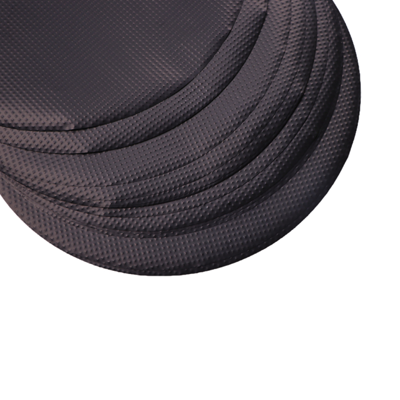
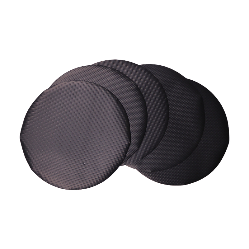
Wafer Spacer Paper ESD (Electrostatic Discharge) is a specialized product designed for use in the semiconductor industry, providing effective protection for wafers during storage, transport, and processing. This paper spacer is engineered to prevent electrostatic discharge, which can damage sensitive semiconductor devices and wafers.

Key Features:

  • ESD Properties: Made from materials that dissipate static electricity, ESD wafer spacer paper helps protect wafers from electrostatic discharge, ensuring the integrity of delicate semiconductor components.
  • High Strength and Durability: Constructed to withstand handling during transportation and processing, this paper is resistant to tearing and damage, providing reliable support for wafers.
  • Precision Thickness: Available in varying thicknesses, ESD wafer spacer paper allows for customizable spacing between wafers, accommodating different wafer types and sizes.
  • Chemical Resistance: This spacer paper is often resistant to various chemicals used in semiconductor fabrication processes, ensuring that it does not degrade or contaminate the wafers.

Wafer Spacer Paper ESD for Semiconductor Manufacturing

  • Prevent Damage: By providing proper spacing, wafer spacers help prevent mechanical damage to wafer surfaces during handling and processing.
  • Enhanced Yield: Reducing the risk of contamination and damage promotes higher yield rates in semiconductor manufacturing, minimizing defects in the final products.
  • Improved Handling: Wafer spacers facilitate easier handling and transport of wafers, streamlining workflows in semiconductor fabrication facilities.
  • Cost-Effective Solution: Investing in quality wafer spacers can result in lower costs associated with wafer damage, rework, and scrap.

Wafer Spacer Paper ESD for Semiconductor Manufacturing

Applications:

  • Semiconductor Manufacturing: Wafer spacers are primarily used in the semiconductor industry during wafer processing steps, including photolithography, etching, and chemical vapor deposition (CVD).
  • Wafer Transport and Storage: These spacers help maintain proper spacing when storing or transporting wafers, protecting them from scratches and contamination.

Submit Your Sourcing Request

We'd like to work with you

Send us a message if you have any questions or request a quote. Our experts will give you a reply within 24 hours and help you select the right valve you want.

Get A Free Quote

All of our products are available for sampling