In semiconductor fabrication, controlling contamination is not just a maintenance task—it’s a critical aspect of yield protection. From sub-micron particles to invisible chemical residues, each type of contamination has a different source and risk profile. Effective mitigation requires understanding these contaminants and where they are most likely to appear, and how to remove them with precision.
Cleanroom wipers are essential in this effort, enabling frontline technicians to clean, absorb, and control residue across the fab.
This article breaks down the use of cleanroom wipers in semiconductor fabs based on two dimensions: contaminant type and contaminant location.
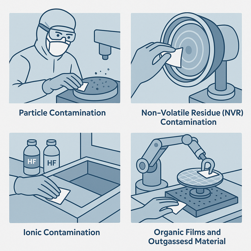
Particle Contamination
A. Lithography Tools (Chucks, Reticle Stages, Aligners)
-
Risk: Dust, skin flakes, airborne fibers, or particles from wafer handling.
-
Why it matters: Particle contamination can disrupt photoresist patterns or cause exposure defects.
-
Wiper strategy: Use sealed-edge microfiber or laser-sealed polyester wipers, pre-wetted with 70% IPA for static dissipation and streak-free removal.
B. Wafer Transfer Robots and Load Ports
-
Risk: Abrasive particle buildup from repetitive motion or mechanical wear.
-
Wiper strategy: Use tough, abrasion-resistant polyester wipers with minimal shedding. Ideal for robotic arms, FOUP docks, and clamps.
C. Gowning Areas and Entry Airlocks
-
Risk: Fibers and particles from human garments, hair, or ambient movement.
-
Wiper strategy: Regular cleaning with general-purpose dry or pre-moistened wipers to remove surface buildup from benches, gloves, or sticky mats.
Non-Volatile Residue (NVR) Contamination
A. Optical Surfaces (Scanner Lenses, Inspection Windows)
-
Risk: NVR from fingerprints, solvent vapors, or outgassing materials.
-
Wiper strategy: Use ultra-clean, non-abrasive microfiber wipers with extremely low NVR levels. Pair with high-purity IPA or lens-safe solvents. Replace gloves before cleaning to avoid transfer.
B. Chamber Surfaces Post-Etch or Deposition
-
Risk: Process residues that may condense or polymerize.
-
Wiper strategy: Use high-absorbency, NVR-certified polyester wipers; often applied during PM with approved solvents (acetone, NMP, or DI water).
C. Packaging and Final Test Sockets
-
Risk: Oils and films from human handling or ambient exposure.
-
Wiper strategy: Neutral pH wipers with low extractables, used dry or with mild solvents to clean trays, sockets, and probe card surfaces.
Ionic Contamination
A. Wet Bench Tools and Chemical Process Zones
-
Risk: Contamination from HF, H2SO4, or base/acid mixtures that leave behind conductive ions.
-
Wiper strategy: Use chemically resistant hydroentangled or knit polyester wipers. Ensure compatibility with acids and proper disposal after use.
B. Wafer Contact Points (Carriers, Boats, Holders)
-
Risk: Ionic leaching or residues from unclean tools.
-
Wiper strategy: Pre-washed and certified wipers with low ion content. Rinse with DI water or process-safe solvents before use in contact-critical steps.
Organic Films and Outgassed Material
A. Process Chamber Interiors
-
Risk: Baked-on films from resist materials, adhesives, or polymer outgassing.
-
Wiper strategy: Tough, textured cleanroom wipers used in combination with mechanical agitation (brush or swab) and compatible cleaning agents.
B. Bonding/Assembly Tables
-
Risk: Glue residue or adhesive mist settling on surfaces.
-
Wiper strategy: Low-lint microfiber wipers with strong absorption properties. In some cases, a double-wipe method (wet + dry) improves effectiveness.
ESD-Sensitive Contamination
A. Tester Stations and Hand Tools
-
Risk: Electrostatic discharge from dry wipers or operator interaction.
-
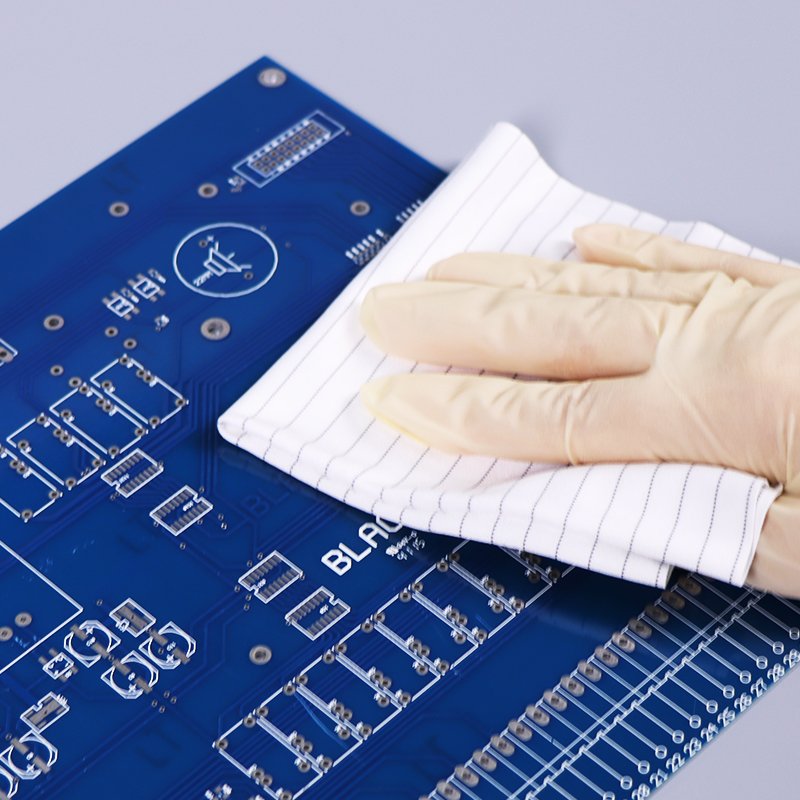
Wiper strategy: ESD-safe cleanroom wipers made with conductive fiber blends or anti-static coatings. Avoid dry friction wiping on sensitive PCB areas.
Practical Guidelines: Matching Wiper to Application
| Contaminant Type | Common Location | Recommended Wiper |
|---|---|---|
| Particles | Reticle stages, robots, and airlocks | Sealed-edge polyester, laser-cut microfiber |
| NVR | Optics, chambers, testing sockets | Ultra-low NVR microfiber, pre-wetted |
| Ionic | Wet benches, carriers | Low-ion content polyester wipers |
| Organic Films | Bonding areas, inner chambers | Textured cleanroom wipers |
| ESD Risk | Probe stations, final testing areas | ESD-safe wipers with static-dissipative fibers |
FAQ: Cleanroom Wipers in Semiconductor Environments
Q1: What’s the difference between sealed-edge and laser-cut wipers?
A: Both are designed to minimize lint. Sealed-edge wipers use heat or ultrasonic sealing for softness and strength, while laser-cut edges offer tighter precision but may have harder fused edges—suitable for critical areas like lithography.
Q2: Can I use general-purpose IPA with cleanroom wipes?
A: Only if it’s high-purity (usually ≥70% semiconductor grade). Industrial-grade IPA can introduce trace contamination.
Q3: How often should cleanroom wipes be replaced?
A: It depends on the task. For critical surfaces (e.g., optics, etch chambers), use single-pass cleaning and replace immediately. For non-critical zones, wipes can be used longer—but always follow your fab’s SOPs.
Q4: What’s a safe way to clean around ESD-sensitive devices?
A: Always use ESD-safe wipers with embedded conductive fibers. Avoid dry wiping; pair with anti-static solvents if possible.
Q5: Are microfiber wipers safe for optics?
A: Yes—if they’re ultra-clean and certified low in NVR. Always pre-wet the wiper and clean in a single direction to avoid scratching or static buildup.
Thank you for considering Myesde for all your cleanroom consumables needs. Contact us today to learn more about our products and how we can support contamination control in your semiconductor facility.
-5.jpg)
