The global semiconductor industry is experiencing unprecedented growth. According to the World Semiconductor Trade Statistics (WSTS), global chip sales are projected to reach USD 701 billion by 2025, marking an 11.2% year-over-year increase and setting a new all-time record. This surge is fueled by high-performance computing, AI-driven applications, and an insatiable demand for memory and logic devices.
However, this rapid expansion has a critical implication: the accelerating need for cleanroom environments. Semiconductor manufacturing is not just a high-tech endeavor—it is a contamination-sensitive process where even a single particle can disrupt an entire production run. As fabs scale up and new facilities come online, cleanroom demand is becoming a cornerstone of the semiconductor supply chain.
Semiconductor Manufacturing: A Cleanroom-Dependent Process
Modern semiconductor fabrication involves processes measured in nanometers, where microscopic contaminants can cause catastrophic defects. Steps such as:
-
Photolithography: Patterning microscopic circuits where a single dust particle can obscure a wafer feature.
-
Thin-Film Deposition: Requiring precise atomic layering without airborne molecular contamination.
-
Etching and Implantation: Demanding strict control over particle size and ionic purity.
These steps are typically performed in ISO Class 3 to ISO Class 5 cleanrooms, where airborne particles ≥0.5 μm are restricted to as few as 35 particles per cubic meter.
As device geometries shrink and extreme ultraviolet (EUV) lithography gains traction, contamination control requirements are becoming even more stringent—driving investments in ultra-clean environments across the globe.
Global Growth Trends and Cleanroom Expansion
Industry forecasts paint a clear picture: cleanroom demand is rising in direct proportion to semiconductor capacity growth.
-
Market Size: WSTS projects global semiconductor sales to hit USD 701 billion in 2025 and continue climbing beyond USD 760 billion in 2026.
-
Fab Construction: SEMI’s World Fab Forecast anticipates more than 1,500 front-end fabs worldwide under construction or in the planning phase through 2026.
-
CapEx Surge: Investments in 300mm fab equipment alone are projected to exceed USD 400 billion by 2027.
Regional Highlights
-
Asia-Pacific: Leading the charge with China, Taiwan, and South Korea spearheading capacity expansions for logic and memory devices.
-
United States: The CHIPS and Science Act is fueling significant domestic fab projects in Arizona, Texas, and Ohio.
-
Europe: Smaller in scale but gaining momentum, particularly in advanced packaging and specialty semiconductor segments.
This aggressive build-out translates into massive demand for cleanroom infrastructure—from facility design and HVAC systems to contamination control products like wipes, garments, and gloves.
Consumables and Contamination Control
Every new cleanroom requires a continuous supply of consumables to maintain its classification and protect processes. The surge in fab construction is amplifying demand for:
-
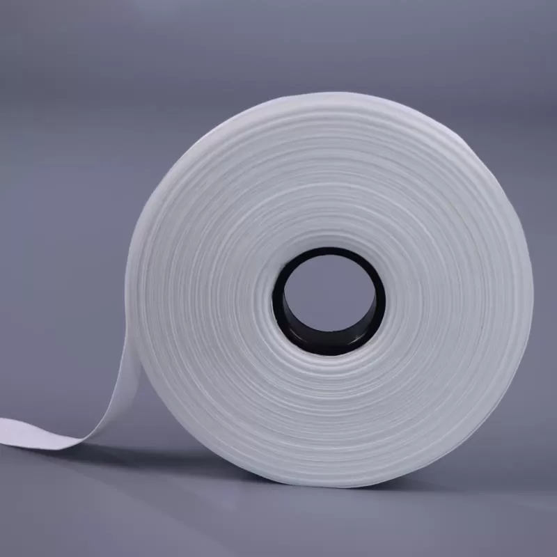
Cleanroom Wipes: High-purity polyester and blended wipes, including low-endotoxin and presaturated options for ISO Class 3–5 environments.
-
Apparel and Gloves: Increased frequency of gowning drives up demand for ESD garments, nitrile gloves, and sterile accessories.
-
ESD and Surface Protection Products: Critical for static-sensitive device handling and contamination prevention.
Studies suggest that consumables account for 20–30% of a cleanroom’s operational costs, making them a strategic focus area for procurement and supply chain resilience.
Key Drivers Behind Consumable Demand
-
Higher ISO Class Standards: Advanced nodes (<5 nm) necessitate ultra-clean wipes and garments that minimize particle release.
-
Automation Growth: While reducing manual contamination risks, automation still requires stringent cleaning protocols and frequent surface wipe-downs.
-
Regulatory Compliance: GMP and ISO 14644 standards demand documented contamination control procedures, boosting the use of certified products.
Challenges and Future Outlook
Cost vs. Cleanliness
Balancing operational budgets with contamination control is a perennial challenge. Cutting corners on cleanroom supplies can result in yield loss far outweighing initial savings. In a leading-edge fab, a single wafer defect could cost thousands of dollars.
Sustainability and Green Cleanrooms
As fabs expand, so does their environmental footprint. Semiconductor leaders like TSMC and Intel have announced ambitious net-zero targets, pushing for:
-
Energy-efficient HVAC and filtration systems
-
Recyclable cleanroom apparel
-
Low-impact wipes and solvent systems
Green cleanroom solutions are no longer optional—they are a competitive differentiator.
ESG and Compliance
ISO 14001 and regional carbon neutrality mandates are reshaping cleanroom design and consumable choices. Vendors capable of delivering eco-friendly, compliant products will hold a distinct advantage.
Market Data Snapshot
| Metric | 2024 Estimate | 2025 Projection |
|---|---|---|
| Global Semiconductor Sales | $630B | $701B (+11.2%) |
| Fab Equipment Spending (300mm) | $350B | $400B+ by 2027 |
| New Fab Projects (2024–2026) | ~1,500 | Expanding |
Sources: WSTS, SEMI World Fab Forecast
Final Thoughts
The semiconductor boom is fueling an equally robust demand for cleanroom infrastructure and consumables. This is not a short-term spike but a structural trend that will define the industry for the next decade.
Companies that align their contamination control strategies with these growth dynamics—investing in advanced cleanroom technologies, high-performance wipes, and sustainable materials—will be best positioned to thrive in this new era of semiconductor manufacturing.